In the absence of confirmation by device specification sheets, SHARP takes no responsibility for any defects that may occur in equipment using any SHARP devices shown in
catalogs, data books, etc. Contact SHARP in order to obtain the latest device specification sheets before using any SHARP device.
1
DESCRIPTION
The LR36685 is a CMOS vertical clock driver and
shutter driver IC for CCD area sensors which
provides the functions to convert the voltage and
impedance from the CMOS level.
FEATURES
∑ Built-in seven circuits
≠ 2-level output :
2 circuits for vertical CCD clock driver
Output voltage level (TYP.) = ≠9 to 0 V
≠ 3-level output :
4 circuits for vertical CCD clock driver
Output voltage level (TYP.) = ≠9 to 0 to +15 V
≠ 2-level output :
1 circuit for shutter driver
Output voltage level (TYP.) = ≠9 to +17 V
∑ Switchable between NTSC (EIA) and PAL (CCIR)
modes
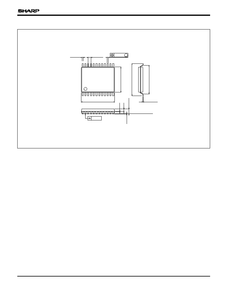
∑ Package :
24-pin SSOP (SSOP024-P-0275)
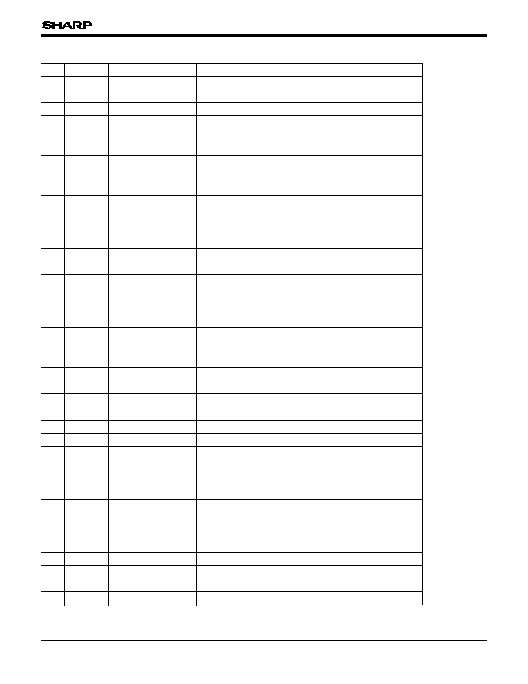
PIN CONNECTIONS
LR36685
LR36685
Vertical Driver IC for
CCD Area Sensors
POFD
VH
1BX
1
24
23
22
21
20
19
18
17
16
15
14
13
V
Mb
V
4X
2
V
L
VH
3AX
3
V
2
GND
4
V
4
V
DD
5
NC
V
3X
6
V
3B
VH
1AX
7
V
3A
V
1X
8
V
1B
V
2X
9
V
1A
OFDX
10
V
Ma
VH
3BX
11
V
H
V
OFDH
12
24-PIN SSOP
TOP VIEW
(SSOP024-P-0275)
LR36685
3
PIN DESCRIPTION
16
GND
Ground
A grounding pin.
PIN NO. SYMBOL
PIN NAME
DESCRIPTION
1
POFD
OFD pulse output
An electronic shutter pulse output.
(high level = V
OFDH
, low level = V
L
)
2
V
Mb
Power supply
A power supply for high level of V
2
and V
4
.
3
V
L
Power supply
A power supply for low level of all output pulses.
4
V
2
Vertical transfer
pulse output 2
A pulse to drive vertical CCD shift register.
Connect to ÿ
V2
.
5
V
4
Vertical transfer
pulse output 4
A pulse to drive vertical CCD shift register.
Connect to ÿ
V4
.
6
NC
No connection
No connection
A pulse to drive vertical CCD shift register.
Connect to ÿ
V3B
.
Vertical transfer
pulse output 3B
V
3B
7
9
V
1B
Vertical transfer
pulse output 1B
A pulse to drive vertical CCD shift register.
Connect to ÿ
V1B
.
8
V
3A
Vertical transfer
pulse output 3A
A pulse to drive vertical CCD shift register.
Connect to ÿ
V3A
.
A pulse to drive vertical CCD shift register.
Connect to ÿ
V1A
.
Vertical transfer
pulse output 1A
V
1A
10
11
V
Ma
Power supply
A power supply for intermediate level of V
1A
, V
1B
, V
3A
and V
3B
.
A power supply for high level of V
1A
, V
1B
, V
3A
and V
3B
.
Power supply
V
H
12
13
VH
1BX
Readout pulse input
1B
A pulse that transfers the charge of the photo-diode to
the vertical shift register.
A vertical transfer pulse input.
Vertical transfer
pulse input 4
V
4X
14
15
VH
3AX
Readout pulse input
3A
A pulse that transfers the charge of the photo-diode to
the vertical shift register.
A vertical transfer pulse input.
Vertical transfer
pulse input 3
V
3X
18
A power supply for input pulses.
Power supply
V
DD
17
19
VH
1AX
Readout pulse input
1A
A pulse that transfers the charge of the photo-diode to
the vertical shift register.
A vertical transfer pulse input.
Vertical transfer
pulse input 1
V
1X
20
22
OFDX
OFD pulse input
An electronic shutter pulse input.
21
V
2X
Vertical transfer
pulse input 2
A vertical transfer pulse input.
A pulse that transfers the charge of the photo-diode to
the vertical shift register.
Readout pulse input
3B
VH
3BX
23
24
V
OFDH
Power supply
A power supply for high level of POFD.

LR36685
5
ELECTRICAL CHARACTERISTICS
DC Characteristics
(V
DD
= +3.3 V, V
H
= +15.0 V, V
L
= ≠9.0 V, V
Ma
= V
Mb
= 0 V, V
OFDH
= +17.0 V, T
A
= +25 ∞C)
Input "Low" voltage
V
IL
Input "High" voltage
V
IH
Input "Low" current
|I
IL
|
|I
IH
|
Output "Low" voltage
V
OL
Output "High" voltage
V
OH
Output "Intermediate" voltage
V
OMLa
V
OMHa
V
OMLb
V
OMHb
Output "Low" current
|I
OL
|
Output "High" current
|I
OH
|
Output "High" current
|I
OFDH
|
Output "Intermediate" current
|I
OMLa
|
|I
OMHa
|
|I
OMLb
|
|I
OMHb
|
R
ONH
R
ONOFH
R
ONM
R
ONL
|I
DD
|
PARAMETER
SYMBOL
CONDITIONS
Input "High" current
V
OFDH
Output "High" voltage
MIN.
0.8V
DD
0.0
1.0
1.0
1.0
1.0
1.0
1.0
1.0
≠0.1
≠0.1
≠0.1
≠0.1
16.9
14.9
20
25
20
TYP.
30
MAX.
1.0
200
V
DD
+ 0.2
0.25V
DD
0.1
0.1
0.1
0.1
≠8.9
2.0
I
OL
< 1 µA
V
IH
= 3.3 V
V
IL
= 0 V
I
OFDH
= 20 mA
I
OH
= 20 mA
V
OMHb
= V
M
+ 0.1 V
V
OMLb
= V
M
≠ 0.1 V
V
OMHa
= V
M
+ 0.1 V
V
OMLa
= V
M
≠ 0.1 V
V
OFDH
= V
OFDH
≠ 0.1 V
V
OH
= V
H
≠ 0.1 V
V
OL
= V
L
+ 0.1 V
I
OMHb
< 1 µA
I
OMLb
< 1 µA
I
OMHa
< 1 µA
I
OMLa
< 1 µA
I
OFDH
< 1 µA
I
OH
< 1 µA
I
OL
= 20 mA
I
OM
= 20 mA
$
$
mA
V
V
V
V
V
V
V
mA
mA
mA
mA
mA
mA
V
V
µA
µA
$
UNIT
$
3
NOTE
3
1, 2, 3
1
2
1, 2, 3
1, 2, 3
µA
µA
200
200
|I
L
|
|I
M
|
µA
µA
200
200
|I
OFDH
|
|I
H
|
2
3
Static current
Output ON resistance
mA
2
2
1
2
1, 2
NOTES :
1. Applied to outputs (V
2
, V
4
).
2. Applied to outputs (V
1A
, V
1B
, V
3A
, V
3B
).
3. Applied to output (POFD).